


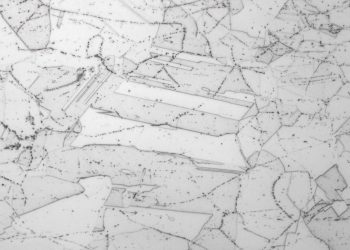
Update: Titanium alloys are typically etched using a grain boundary etchant such Kroll’s or 2% HF. In the case of alpha case evaluations, a tint etch such as ammonium fluoride is used to provide greater contrast between the alpha...
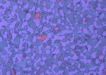
Alpha-beta titanium alloys are commonly used in aerospace applications where high strength and low weight are key performance drivers. Alpha beta titanium alloys are capable of matching the strength of high strength steels while having nearly half the mass....
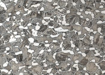
Inconel 600 and 625 are both solid-solution strengthened nickel chromium alloys. They are used for their corrosion resistance more than their high temperature counterparts. They are commonly used in applications where corrosion and strength are of concern such as...